Silicon wafers have been utilized richly in microelectronics and MEMS as a stage for manufacture. A fascinating variety of the standard Diced silicon wafer with a dry oxide coating is the SOI substrate. To deliver these wafers, two silicon wafers are reinforced together, utilizing silicon dioxide of around 1�2 �m thickness as a bond layer. One of the silicon wafers is weakened to a thickness of 10�50 �m.
Read MoreBlog #Diced silicon wafer with a dry oxide coating
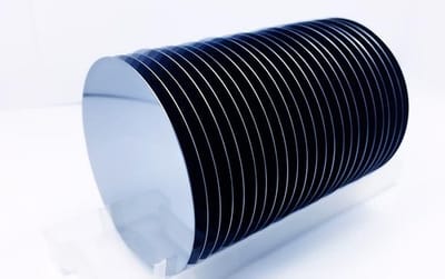
Silicon wafers have been utilized richly in microelectronics and MEMS as a stage for manufacture. A fascinating variety of the standard Diced silicon wafer with a dry oxide coating is the SOI substrate. To deliver these wafers, two silicon wafers are reinforced together, utilizing silicon dioxide of around 1�2 �m thickness as a bond layer. One of the silicon wafers is weakened to a thickness of 10�50 �m.
Read More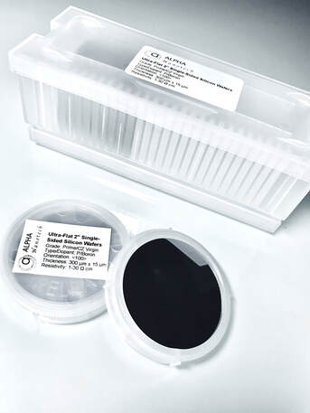
We give warm oxide wafer in measurement from 2" to 12 " , we generally pick prime evaluation and imperfection free P-type Boron-doped 200nm SiO2 thermal oxide wafer as substrate for developing high consistency warm oxide layer to meet your particular necessities . Reach us for additional data on cost and conveyance time.
Read More
Innovative tools and materials such as agate grinding mortar and pestles, prime-grade 4-inch silicon wafers, and many more are important resources that are used in scientific research and industrial applications.
Read MorePrime-Grade 4 Inch Silicon Wafer can be utilized for everything, from delivering semiconductor gadgets to building electronic gadgets. They're the most elevated evaluation of silicon wafers. They're otherwise called Gadget quality due to their capacity to offer severe resistivity specs, astounding quality, expanded life expectancy, and the profoundly cleaned and clean wafer surface.
Read MorePrime-Grade 4 Inch Silicon Wafer can be utilized for everything, from delivering semiconductor gadgets to building electronic gadgets. They're the most elevated evaluation of silicon wafers. They're otherwise called Gadget quality due to their capacity to offer severe resistivity specs, astounding quality, expanded life expectancy, and the profoundly cleaned and clean wafer surface.
Read MoreWe give warm oxide wafer in measurement from 2" to 12 " , we generally pick prime evaluation and imperfection free P-type Boron-doped 200nm SiO2 thermal oxide wafer as substrate for developing high consistency warm oxide layer to meet your particular necessities . Reach us for additional data on cost and conveyance time.
Read MoreDespite the most recent examination progress of PMMA nanoparticles, the flawed properties of last nanocomposite and the absence of long haul clinical proof tending to their presentation limit their wide clinical use. A decisive association between nanoparticle size or expansion technique and nanocomposite properties couldn't be set up.
Read More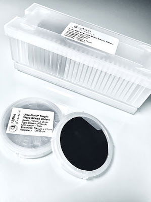
We give warm oxide wafer in measurement from 2" to 12 " , we generally pick prime evaluation and imperfection free P-type Boron-doped 200nm SiO2 thermal oxide wafer as substrate for developing high consistency warm oxide layer to meet your particular necessities . Reach us for additional data on cost and conveyance time.
Read More
Silicon wafers have been utilized richly in microelectronics and MEMS as a stage for manufacture. A fascinating variety of the standard Diced silicon wafer with a dry oxide coating is the SOI substrate. To deliver these wafers, two silicon wafers are reinforced together, utilizing silicon dioxide of around 1�2 �m thickness as a bond layer. One of the silicon wafers is weakened to a thickness of 10�50 �m.
Read More
We give warm oxide wafer in measurement from 2" to 12 " , we generally pick prime evaluation and imperfection free P-type Boron-doped 200nm SiO2 thermal oxide wafer as substrate for developing high consistency warm oxide layer to meet your particular necessities . Reach us for additional data on cost and conveyance time.
Read More