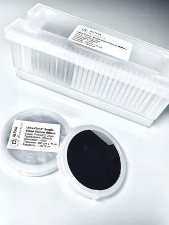
We give warm oxide wafer in measurement from 2" to 12 " , we generally pick prime evaluation and imperfection free P-type Boron-doped 200nm SiO2 thermal oxide wafer as substrate for developing high consistency warm oxide layer to meet your particular necessities . Reach us for additional data on cost and conveyance time.
Read MoreBlog #Diced silicon wafer with a dry oxide coating
Silicon wafers have been utilized richly in microelectronics and MEMS as a stage for manufacture. A fascinating variety of the standard Diced silicon wafer with a dry oxide coating is the SOI substrate. To deliver these wafers, two silicon wafers are reinforced together, utilizing silicon dioxide of around 1�2 �m thickness as a bond layer. One of the silicon wafers is weakened to a thickness of 10�50 �m.
Read MoreSilicon wafers have been utilized richly in microelectronics and MEMS as a stage for manufacture. A fascinating variety of the standard Diced silicon wafer with a dry oxide coating is the SOI substrate. To deliver these wafers, two silicon wafers are reinforced together, utilizing silicon dioxide of around 1�2 �m thickness as a bond layer. One of the silicon wafers is weakened to a thickness of 10�50 �m.
Read More
Amine-terminated magnetic silica beads are composite particles that combine the magnetic properties of iron oxide with the surface functionality of amine groups. These beads typically consist of a core of magnetic iron oxide encapsulated within a silica shell, and the surface is modified with amine (-NH2) groups. This unique combination of magnetic and amine functionalities opens up a wide range of possibilities in various biomedical applications.
Read More
Get the highest quality silicon wafer with a dry oxide coating from Diced for your next project! Our wafers are designed for maximum performance and durability, letting you create the perfect device with precision. With our easy-to-use cutting process, you'll get perfect cuts every time. Plus, our dry oxide coating ensures your projects will remain safe and secure. Get the best in silicon wafer technology with Diced today!
Read MoreSilicon wafers have been utilized richly in microelectronics and MEMS as a stage for manufacture. A fascinating variety of the standard Diced silicon wafer with a dry oxide coating is the SOI substrate. To deliver these wafers, two silicon wafers are reinforced together, utilizing silicon dioxide of around 1–2 µm thickness as a bond layer. One of the silicon wafers is weakened to a thickness of 10–50 µm.
Read More
Silicon wafers have been utilized richly in microelectronics and MEMS as a stage for manufacture. A fascinating variety of the standard Diced silicon wafer with a dry oxide coating is the SOI substrate. To deliver these wafers, two silicon wafers are reinforced together, utilizing silicon dioxide of around 1–2 µm thickness as a bond layer. One of the silicon wafers is weakened to a thickness of 10–50 µm.
Read MoreSilicon wafers have been utilized richly in microelectronics and MEMS as a stage for manufacture. A fascinating variety of the standard Diced silicon wafer with a dry oxide coating is the SOI substrate. To deliver these wafers, two silicon wafers are reinforced together, utilizing silicon dioxide of around 1–2 µm thickness as a bond layer. One of the silicon wafers is weakened to a thickness of 10–50 µm.
Read MoreSilicon wafers have been utilized richly in microelectronics and MEMS as a stage for manufacture. A fascinating variety of the standard Diced silicon wafer with a dry oxide coating is the SOI substrate. To deliver these wafers, two silicon wafers are reinforced together, utilizing silicon dioxide of around 1–2 µm thickness as a bond layer.
Read More
Silicon wafers have been utilized richly in microelectronics and MEMS as a stage for manufacture. A fascinating variety of the standard Diced silicon wafer with a dry oxide coating is the SOI substrate. To deliver these wafers, two silicon wafers are reinforced together, utilizing silicon dioxide of around 1–2 µm thickness as a bond layer. One of the silicon wafers is weakened to a thickness of 10–50 µm.
Read More