Silicon wafers have been utilized richly in microelectronics and MEMS as a stage for manufacture. A fascinating variety of the standard Diced silicon wafer with a dry oxide coating is the SOI substrate. To deliver these wafers, two silicon wafers are reinforced together, utilizing silicon dioxide of around 1–2 µm thickness as a bond layer. One of the silicon wafers is weakened to a thickness of 10–50 µm.
Read MoreBlog #Diced silicon wafer with a dry oxide coating

Silicon wafers have been utilized richly in microelectronics and MEMS as a stage for manufacture. A fascinating variety of the standard Diced silicon wafer with a dry oxide coating is the SOI substrate. To deliver these wafers, two silicon wafers are reinforced together, utilizing silicon dioxide of around 1–2 µm thickness as a bond layer. One of the silicon wafers is weakened to a thickness of 10–50 µm.
Read More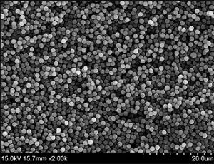
Magnetic Silica Nanoparticles & Microspheres with various properties, for example, unique center structures, sizes, coatings, and surface adjustments are accessible industrially. Studies have been directed to comprehend the part of these properties for ligand fishing tests. Here we assessed, unexpectedly, the impact of MB size on the ligand fishing examine for acetylcholinesterase from Electrophorus electricus (AChE).
Read More
Silicon wafers have been utilized richly in microelectronics and MEMS as a stage for manufacture. A fascinating variety of the standard Diced silicon wafer with a dry oxide coating is the SOI substrate. To deliver these wafers, two silicon wafers are reinforced together, utilizing silicon dioxide of around 1–2 µm thickness as a bond layer. One of the silicon wafers is weakened to a thickness of 10–50 µm.
Read More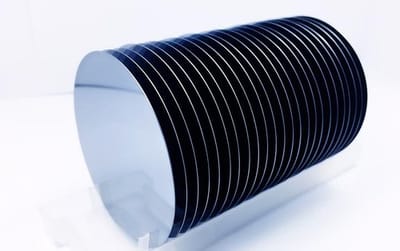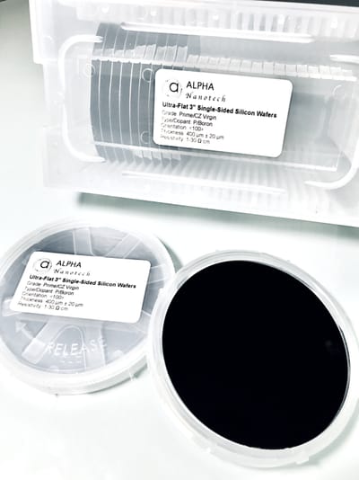
We give warm oxide wafer in measurement from 2" to 12 " , we generally pick prime evaluation and imperfection free P-type Boron-doped 200nm SiO2 thermal oxide wafer as substrate for developing high consistency warm oxide layer to meet your particular necessities . Reach us for additional data on cost and conveyance time.
Read More
Prime-Grade 4 Inch Silicon Wafer can be utilized for everything, from delivering semiconductor gadgets to building electronic gadgets. They're the most elevated evaluation of silicon wafers. They're otherwise called Gadget quality due to their capacity to offer severe resistivity specs, astounding quality, expanded life expectancy, and the profoundly cleaned and clean wafer surface.
Read More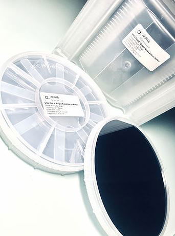
We give warm oxide wafer in measurement from 2" to 12 " , we generally pick prime evaluation and imperfection free P-type Boron-doped 200nm SiO2 thermal oxide wafer as substrate for developing high consistency warm oxide layer to meet your particular necessities . Reach us for additional data on cost and conveyance time.
Read More
We give warm oxide wafer in measurement from 2" to 12 " , we generally pick prime evaluation and imperfection free P-type Boron- doped 200nm SiO2 thermal oxide wafer as substrate for developing high consistency warm oxide layer to meet your particular necessities . Reach us for additional data on cost and conveyance time.
Read More
We give warm oxide wafer in measurement from 2" to 12 " , we generally pick prime evaluation and imperfection free P-type Boron-doped 200nm SiO2 thermal oxide wafer as substrate for developing high consistency warm oxide layer to meet your particular necessities . Reach us for additional data on cost and conveyance time.
Read More