Must-know facts about P-type Boron-doped 200nm SiO2 thermal oxide wafer?
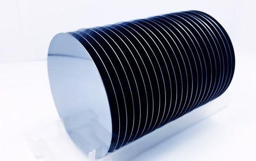
Prime-grade 4 inch silicon wafer are open in a combination of assessments, from prime assessment wafers to InP recuperate wafers—they are gathered by their quality. Every assessment of silicon also has its properties and applications.
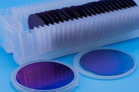
P-type Boron-doped 200nm SiO2 thermal oxide wafer is molded on revealed silicon surface at a raised temperature inside seeing an oxidant; the method is called warm oxidation. Warm oxide is commonly filled in an even chamber warmer, at a temperature range from 900°C ~ 1200°C, using either a "Wet" or "Dry" advancement technique. Warm oxide is such a "created" oxide layer, stood out from CVD saved oxide layer, it has a higher consistency, and higher dielectric quality, and it is an extraordinary dielectric layer as a separator. Deepest silicon-based devices, the warm oxide layer anticipates an enormous capacity to pacify the silicon exterior to go about as doping hindrances as well as as surface dielectrics. SWI gives warm oxide wafer in estimation from 2" to 12 ", we by and large pick prime assessment and flaw free P-type Boron-doped 200nm SiO2 warm oxide wafer as a substrate for growing high consistency warm oxide layer to meet your specific necessities. Contact us for extra information on expense and transport time.
Prime Grade
Prime-Grade 4 Inch Silicon Wafer can be used for everything, from conveying semiconductor contraptions to building electronic devices. They're the most raised assessment of silicon wafers. They're generally called Gadget quality because of their ability to offer extreme resistivity specs, bewildering quality, extended future, and the significantly cleaned and clean wafer surface. They're all the more exorbitant diverged from various types of assessments; notwithstanding, their quality and execution legitimize their cost.