What is P-type Boron-doped 200nm SiO2 thermal oxide wafer?
Silicon wafers are accessible in an assortment of evaluations, from prime evaluation wafers to InP recover wafers—they're grouped by their quality. Each evaluation of silicon additionally has its properties and applications. We can give a breakdown here to the diverse silicon wafer grades and every one of their applications.
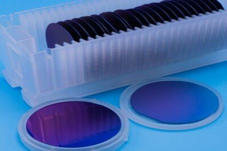
Warm oxide or silicon dioxide layer is shaped on uncovered silicon surface at raised temperature within the sight of an oxidant; the technique is called warm oxidation. Warm oxide is typically filled in an even cylinder heater , at temperature range from 900°C ~ 1200°C , utilizing either a "Wet" or "Dry" development strategy . Warm oxide is a sort of "developed" oxide layer , contrasted with CVD saved oxide layer , it has a higher consistency, and higher dielectric quality , it is a great dielectric layer as a separator . In most silicon-based gadgets, warm oxide layer assume a significant function to conciliate the silicon surface to go about as doping obstructions and as surface dielectrics . SWI gives warm oxide wafer in measurement from 2" to 12 " , we generally pick prime evaluation and imperfection free P-type Boron-doped 200nm SiO2 thermal oxide wafer as substrate for developing high consistency warm oxide layer to meet your particular necessities . Reach us for additional data on cost and conveyance time.
 P-type Boron-Doped 200nm SiO2 Thermal Oxide Wafer
Prime Grade
Prime-Grade 4 Inch Silicon Wafer can be utilized for everything, from delivering semiconductor gadgets to building electronic gadgets. They're the most elevated evaluation of silicon wafers. They're otherwise called Gadget quality due to their capacity to offer severe resistivity specs, astounding quality, expanded life expectancy, and the profoundly cleaned and clean wafer surface. They're more costly contrasted with different kinds of evaluations, however their quality and execution legitimize their expense.